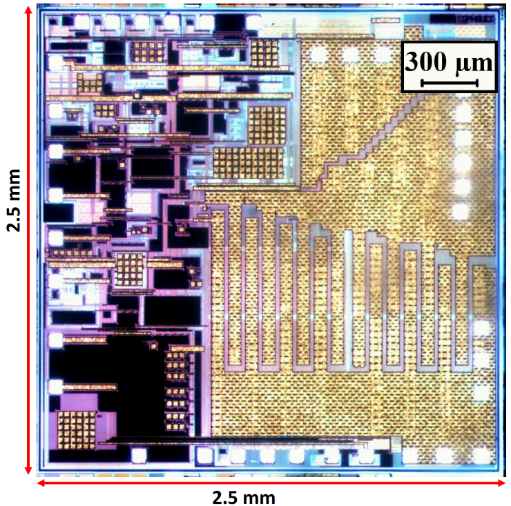
Chip Gallery

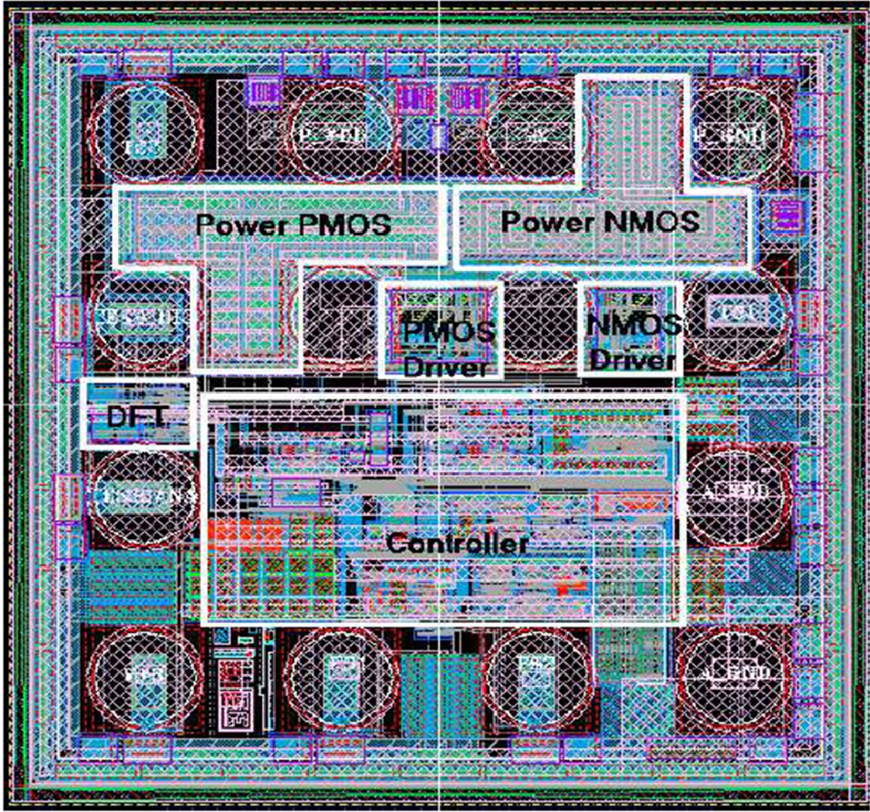
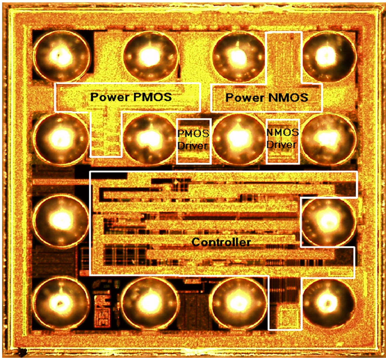
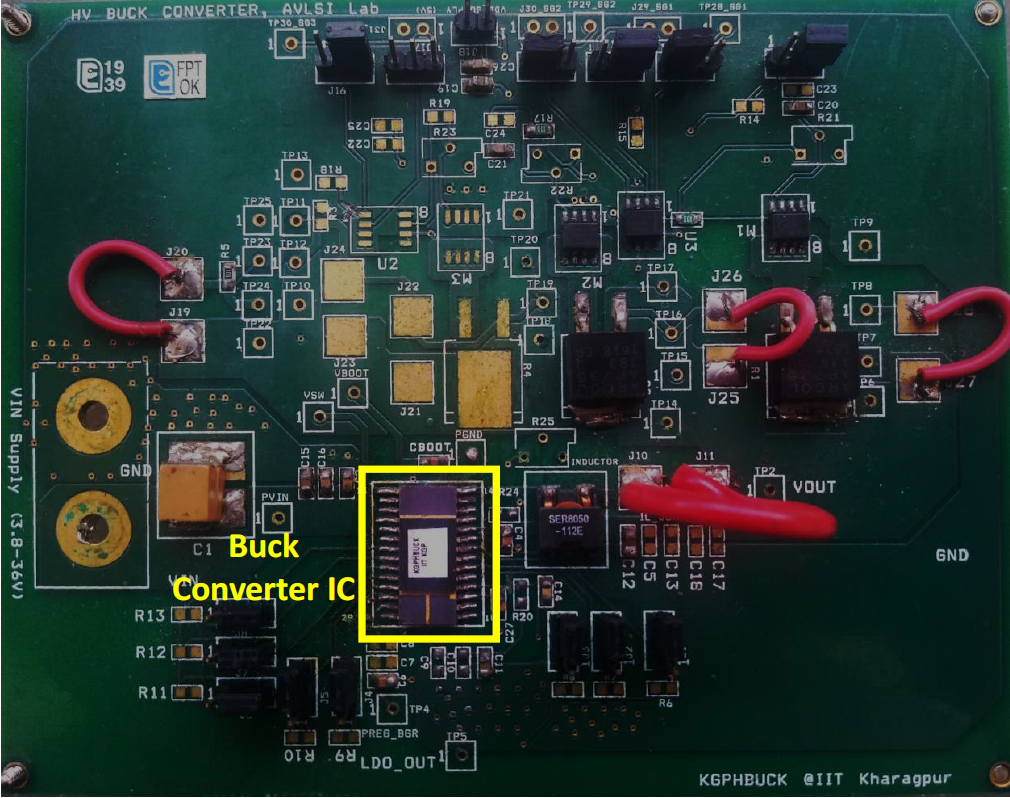
    Design and Implementation of a Wide Input Voltage Buck Converter Chip for Automotive Applications


    Abstract: This work presents the design and implementation of an integrated high voltage buck converter circuit for automotive applications, supporting a wide input (3.8-36 V) to output (3.3 V) step-down ratio with a full load requirement of 3.3 A. The major contributions of this work are (i) the design and implementation of an on-chip bias generator to generate a regulated low voltage supply, (ii) a high voltage level shifter to communicate signals between the high voltage power stage and the low voltage controller, (iii) a voltage-emulated peak current sensing method and (iv) an adaptive switching frequency controller with a re-configurable compensation. The proposed adaptively biased low dropout regulator generates a 5 V regulated voltage from 5.5-36 V input with 5 µA standby quiescent current for supplying 10 µA-20 mA load current. With a 0-20 mA load step and 1 µF output capacitor, undershoot of 40 mV and overshoot of 55 mV are achieved experimentally. The proposed high voltage level shifter has a strengthened pull-up path during transients, which enables it to overcome the limited speed of operation and a high switching power loss due to a large crowbar current in the conventional designs. The voltage-emulated peak current sensing method adopted in this work is faster and more accurate compared to conventional schemes that are limited in sensing speed by the bandwidth of the Op-Amp based feedback mechanisms. The error voltage emulates the inductor peak current for current comparison and dynamically adjusts its value with the load current. The efficacy of the proposed scheme is extended to implement. over-current protection for the converter with an in-built maximum current limiter which restricts the maximum sense-FET current. A dual switching frequency (2.1 MHz, 1.05 MHz) controller, determined by the input voltage level, is presented in this work to meet the stringent requirement of the minimum on/off time over a wide input supply range for the buck converter. A re-configurable compensation achieved by tuning the feedback resistances, optimizes the transient response, in contrast to the conventional fixed compensator circuit where the loop bandwidth of the converter is optimized mainly at the lowest switching frequency. The proposed wide input voltage automotive buck converter design is implemented in a high voltage 0.18 µm Bipolar-CMOS-DMOS technology and validated with post-layout simulation results. A settling time of 70 µs is observed for a load transient of 3.3 A-1 mA with an undershoot and overshoot of 81 mV and 75 mV respectively using on-chip filter components of L = 1.1 µH and C = 47 µF. The converter shows the load and line regulations of 24.54 mV/A and 0.97 mV/V respectively. The peak power efficiency is 88.6% at 3.3 A at 13.5 V supply.


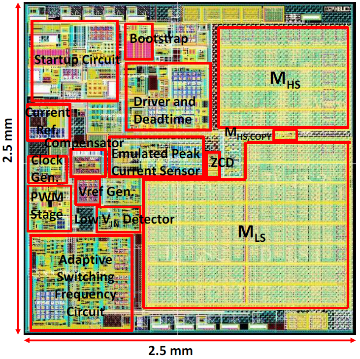
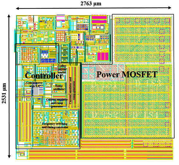
    A Valley-Sensed Emulated Peak Current Controlled Buck Converter for Automotive Applications


    Abstract: In automotive applications, the input voltage varies widely during cold cranking and load dumping conditions. However, a regulated voltage is required to provide the supply of various automotive electronic components such as microcontrollers, dashboards, LED displays, etc. So, a high-voltage DC-DC converter is essential to bridge the gap between the battery and the supply of the automotive electronic components. This dissertation discusses various challenges to implement a DC-DC buck converter for automotive applications, where one of the key challenges is to protect the devices from high voltage stress. The proposed converter architecture adopts a valley-sensed emulated peak current-mode control mechanism to eliminate the issue of the voltage stress along with reducing the design complexity of the current sensing block. Moreover, this architecture greatly reduces the minimum on-time requirement of the converter to achieve a very low duty cycle. Additionally, the issue of sub-harmonic oscillations in the current-mode controller has been resolved by using an adaptive slope compensation. The proposed converter has been designed in a 0.18 µm Bipolar-CMOS-DMOS (BCD) process technology with a maximum load current of 3.3 A. The input operating voltage of the converter ranges from 4 V to 36 V with an output voltage of 3.3 V. The converter operates at dual switching frequencies (2.1 MHz and 1.05 MHz), determined by the input voltage level. In the post-layout simulation results, a fast settling time of ~30 µs is observed when the load switches from 100 mA to 3.3 A and vice-versa using off-chip filter components of L = 1.1 µH and C = 40 µF. The overshoot and undershoot are recorded as 98 mV and 120 mV respectively. The converter shows a load regulation of 29.37 µV/mA, and a line regulation of 2.13 µV/mV. The output ripple value is nearly 9-11 mV with an ESR of 10 mohm. The proposed converter achieves a minimum on-time of 28 ns and a minimum off-time of 120 ns, thanks to its simplified architecture. The peak power efficiency is 93.63% at 2 A. .


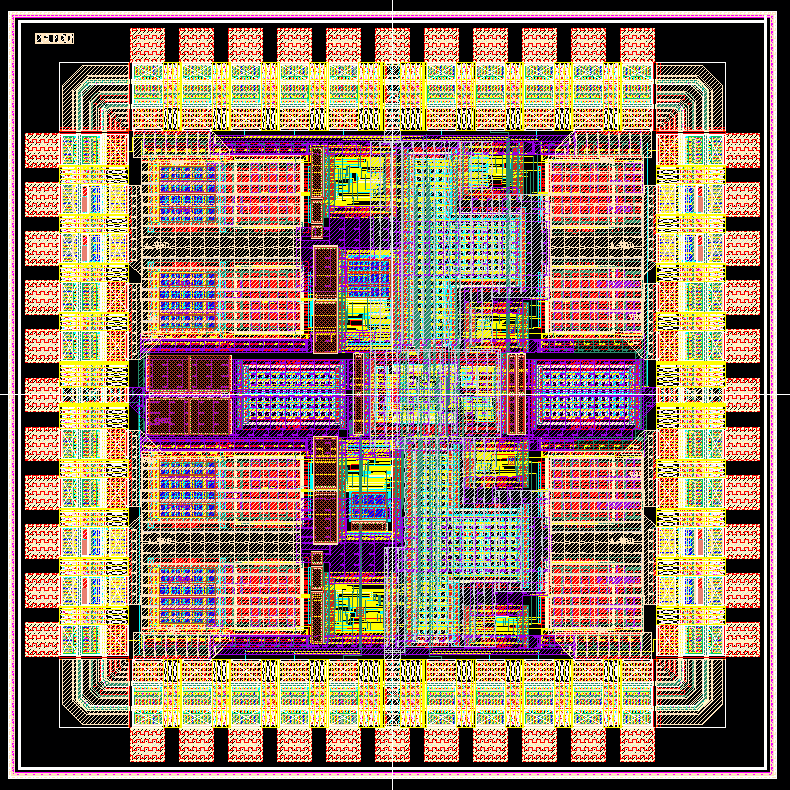
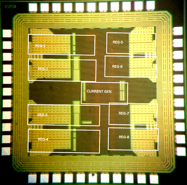
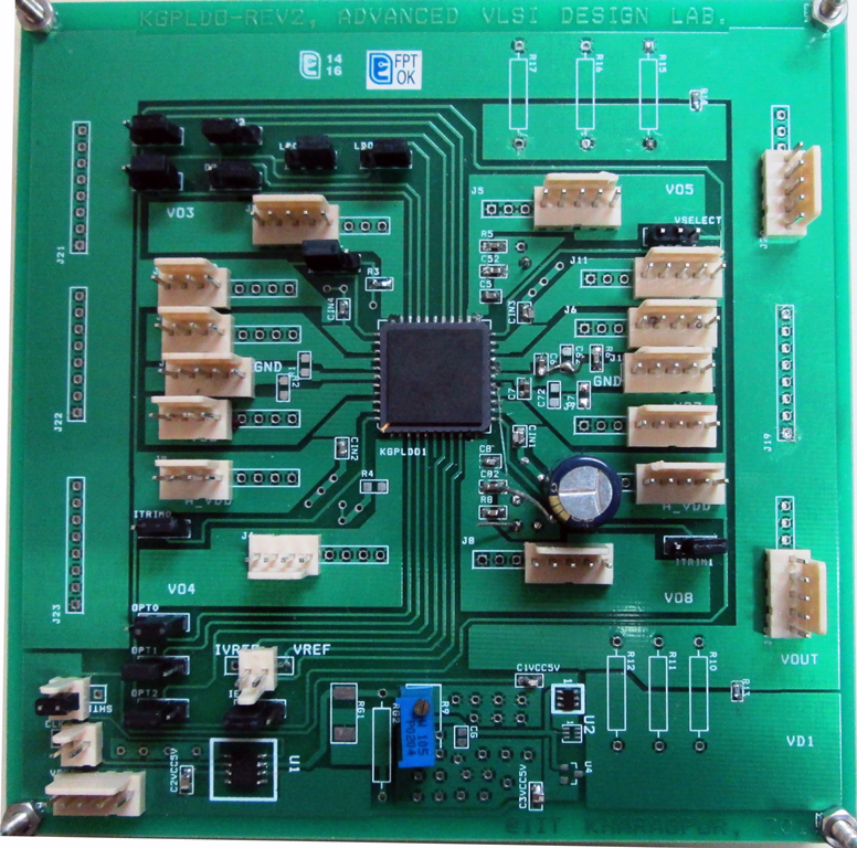
    Design and Analysis of Self-Compensated Low Dropout Regulators


    Abstract: Today's feature-laden portable electronic devices require multiple low dropout regulators (LDRs). Based on the presence of an off-chip output capacitor, the LDRs are classified into two categories i.e., with-capacitor LDR (WC-LDR) and capacitor-less LDR (CL-LDR). In this work, we have explored both the above categories of the LDR. To improve the battery lifetime, the main objective is to minimize the quiescent current while maintaining a fast transient response. In view of this, the adaptive biasing scheme is primarily adopted. All the topologies are implemented in 0.18 µm CMOS technology.
    To start with, the widely used nested Miller compensated (NMC) architecture is revisited to identify the various design trade-offs and limitations. A systematic design procedure is also proposed to optimize various dynamic performances. After that, a self-compensated architecture that has many advantages over the NMC one is developed. Using this architecture a generic, adaptively biased LDR (AB-LDR) topology which is suitable for both the with-capacitor and capacitor-less conditions is proposed. A power efficient enhanced current mirror (ECM) buffer is proposed in particular to the WC-LDR to expand the loop bandwidth of the regulator. We have also proposed a dynamically slew enhanced adaptive bias (DSE-AB) scheme to improve the dynamic response further in the WC-LDR. Finally, while applying the DSE-AB scheme in the CL-LDR, an issue of low momentary damping is observed as various system poles move at different rates during transient. A current-limited DSE-AB scheme is explored to increase the momentary damping in capacitor-less condition. All the topologies are developed, backed with theoretical analysis and validated with simulation and experimental results when they are implemented in a standard 0.18 µm CMOS technology. Apart from exploring different topologies, this work has also proposed advancement in small signal analysis of the adaptively biased LDR (AB-LDR) topologies.


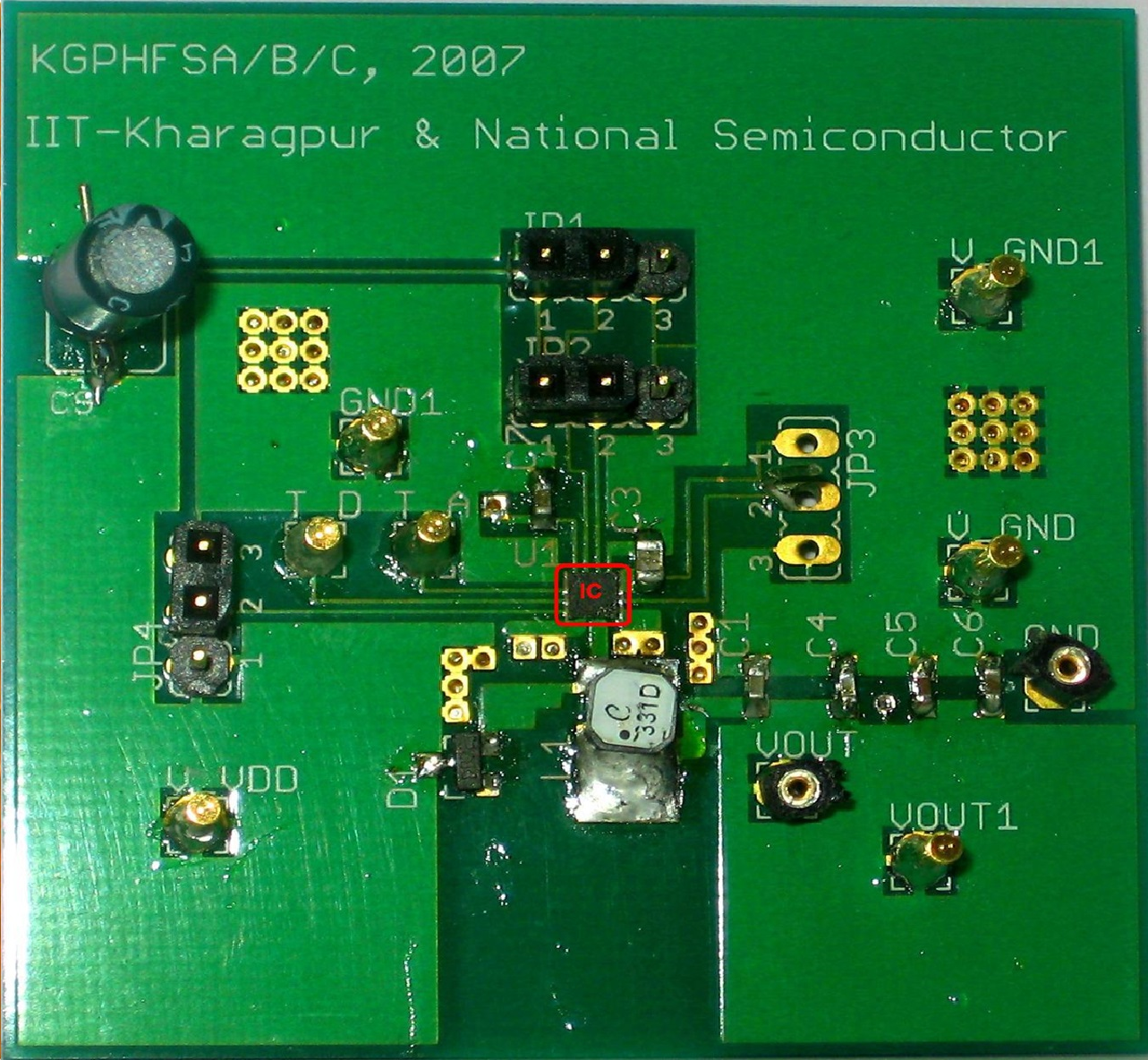
    Design of a 20 MHz DC-DC Buck Converter with 84% Efficiency for Portable Applications


    Abstract: This work presents the design and implementation of a 20 MHz voltage mode DC-DC buck converter with high power efficiency. The power efficiency has been improved by minimizing the short circuit current in the driver stage. At the same time, a high gain, wide-band error amplifier topology with reduced current consumption, improves various dynamic performance parameters such as settling time, load and line regulations of the converter. A prototype of a 20 MHz DC-DC buck converter has been implemented and fabricated in 0.5 µm Bi-CMOS process with a maximum of 600 mA load current driving capability in the input voltage range of 2.7-5.5 V which is suitable for single-cell lithium-ion (Li-Ion) battery operated portable applications. A reasonably good settling time of 10 µs is observed in the measured result with off-chip filter components of L=270 nH, C=1.6 µF. The measured value of load regulation and line regulation are 1.6 mV/A and 3 mV/V respectively. A maximum of 84% power efficiency is achieved at 2.7 V to 1.2 V conversion. A very low form factor of 2.5 mm X 2.5 mm X 0.7 mm, has been achieved by using apower flip-chip packaging technology.